
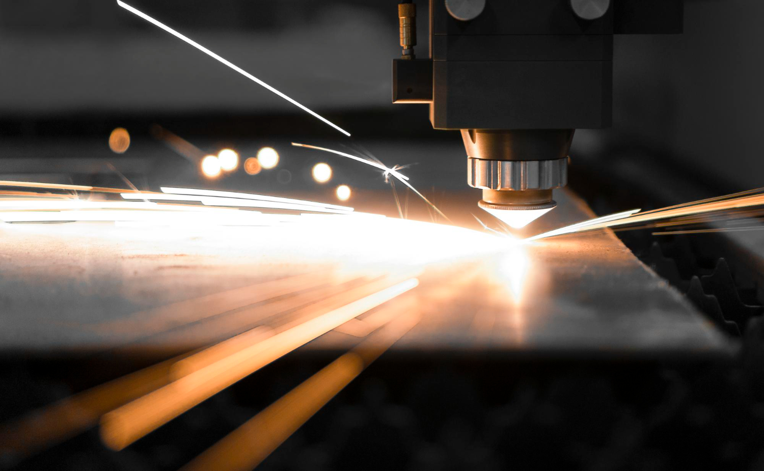
Laser precision micromachining technology is widely used in micron-level cutting, drilling, and marking of hard and brittle materials such as silicon, silicon carbide, and ceramics. The core of this industry lies in enhancing the chip output efficiency and stability of advanced packaging.
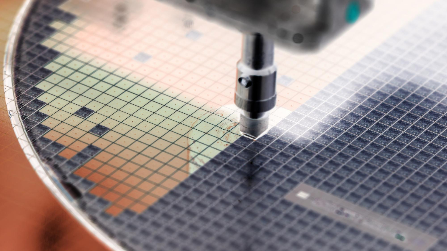
Wafer dicing and drilling: Utilizing femtosecond laser technology for SiC (silicon carbide) cutting and TSV (through-silicon via) technology to meet the stringent requirements of high-performance computing chips for heat dissipation and precision.
Advanced packaging: Laser technology is applied to redistribution layers (RDL), wafer marking, and laser deflash in advanced packaging.
TGV (Through-Glass Via): Ingentec Corporation specializes in laser modification and drilling of thick glass substrates, focusing on the development of glass substrates required for advanced packaging.
Non-contact precision processing: Laser technology offers advantages including high precision, low energy consumption, and no tool wear, making it particularly well-suited for miniaturized electronic components – a key trend in future electronics.
Ultrashort pulse laser “cold processing”: Ultrashort pulse lasers can reduce the heat-affected zone and prevent thermal damage to sensitive semiconductor dies, improving packaging quality.
